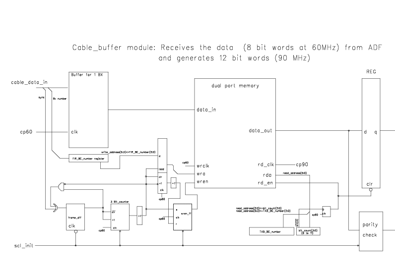
In the new scheme:
| Action | address[5..3] | address[2..0] |
| Write |
ADF_BC_number[2..0] (from ADF input data) |
bit number of data (0-7) (this is generated by a 3-bit counter clocked at 60 MHz) |
| Read |
TAB_BC_number[2..0] (reconstructed from SCL signals) |
bit number of data from DPRAM (0-7) output data bits 8-11 are added to the end of this stream, set to 0 (generated by a 4-bit counter clocked at 90 MHz) |
A block diagram of the synchronization scheme is shown below.
(A ps version is available here.)