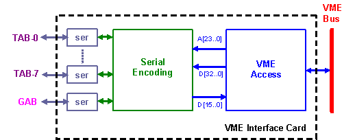
VME accesses to the TABs and GAB are made via the
VME Interface board (VMEI)
that translates VME addresses and data to
serial data sent to the TABs and GAB on separate cables consisting of
6 data pairs using LVDS protocol.
A similar cable
and connector
is used for this transmission as is used for
ADF-to-TAB data
transmission.
The only difference is that three 5-pin rows are used
for the VMEI data rather than four 5-pin rows for the ADF-to-TAB
cables.
| Bits | Name | Description |
| 23..19 | ga[4..0] | VME slot address |
| 18..15 | module[3..0] | Module in TAB crate
|
| 14..11 | chip[3..0] | Chip on Module
|
| 10..07 | group[3..0] | memory group |
| 06..04 | sub[3..1] | reserved for sequences to reduce latency |
| Pair | Name | Description |
| 1 | ser_clk | clock for serial transmission |
| 2 | ser_frm_in | frame & destination chip for writes
|
| 3 | ser_addr_in | address in chip for input data (16-bit) |
| 4 | ser_data_in | data to TAB (16-bit) |
| 5 | ser_frm_out | marks 1st bit of 16-bit output data |
| 6 | ser_data_out | data from TAB (16-bit) |
The LVDS serial lines will run at 15 MHz. The limit is actually from the data bus to the FPGAs on the TAB. This means that typical transfer times will be:
| Transfer | Size | Total Time |
| Firmware Download | ~6 MBytes/chip | ~10 sec |
| TAB Online Monitoring 16-bit Sum(Et) and Sum(Et2) for each TT |
1280 Bytes/TAB | ~5.5 ms |