ADF to TAB Cabling
updated: 29-Nov-06
Index
Mapping of Channels to Physical Eta
Mapping of channel number to physical TT eta is done differently for
TAB chips 0-4 and 5-9 because of the way BLS signals are processed in
the ADFs.
ADF Channel Link Signal Connections
to a Single TAB SW Chip
| |
ADF i-1 : Output A
|
ADF i : Output B
|
ADF i+1 : Output C
|
Relative TT
[eta,phi]
|
ADF i-1
[out.chan]
|
Cable Pair
[pair.bit]
|
TAB SW Chip
[input]
|
ADF i
[out.chan]
|
Cable Pair
[pair.bit]
|
TAB SW Chip
[input]
|
ADF i+1
[out.chan]
|
Cable Pair
[pair.bit]
|
TAB SW Chip
[input]
|
| EM[0,0] |
A.0 |
0.0 |
|
B.0 |
0.0 |
E:20 |
C.0 |
0.0 |
E:24 |
| HD[0,0] |
A.1 |
0.1 |
|
B.1 |
0.1 |
H:20 |
C.1 |
0.1 |
H:24 |
| EM[0,1] |
A.2 |
0.2 |
|
B.2 |
0.2 |
E:21 |
C.2 |
0.2 |
E:25 |
| HD[0,1] |
A.3 |
0.3 |
|
B.3 |
0.3 |
H:21 |
C.3 |
0.3 |
H:25 |
| EM[0,2] |
A.4 |
0.4 |
E:18 |
B.4 |
0.4 |
E:22 |
C.4 |
0.4 |
E:26 |
| HD[0,2] |
A.5 |
0.5 |
H:18 |
B.5 |
0.5 |
H:22 |
C.5 |
0.5 |
H:26 |
| EM[0,3] |
A.6 |
3.0 |
E:19 |
B.6 |
3.0 |
E:23 |
C.6 |
3.0 |
|
| HD[0,3] |
A.7 |
3.1 |
H:19 |
B.7 |
3.1 |
H:23 |
C.7 |
3.1 |
|
| |
|
|
|
| EM[1,0] |
A.8 |
1.0 |
|
B.8 |
1.0 |
E:29 |
C.8 |
1.0 |
E:33 |
| HD[1,0] |
A.9 |
1.1 |
|
B.9 |
1.1 |
H:29 |
C.9 |
1.1 |
H:33 |
| EM[1,1] |
A.10 |
1.2 |
|
B.10 |
1.2 |
E:30 |
C.10 |
1.2 |
E:34 |
| HD[1,1] |
A.11 |
1.3 |
|
B.11 |
1.3 |
H:30 |
C.11 |
1.3 |
H:34 |
| EM[1,2] |
A.12 |
1.4 |
E:27 |
B.12 |
1.4 |
E:31 |
C.12 |
1.4 |
E:35 |
| HD[1,2] |
A.13 |
1.5 |
H:27 |
B.13 |
1.5 |
H:31 |
C.13 |
1.5 |
H:35 |
| EM[1,3] |
A.14 |
3.2 |
E:28 |
B.14 |
3.2 |
E:32 |
C.14 |
3.2 |
|
| HD[1,3] |
A.15 |
3.3 |
H:28 |
B.15 |
3.3 |
H:32 |
C.15 |
3.3 |
|
| |
|
|
|
| EM[2,0] |
A.16 |
2.0 |
|
B.16 |
2.0 |
E:38 |
C.16 |
2.0 |
E:42 |
| HD[2,0] |
A.17 |
2.1 |
|
B.17 |
2.1 |
H:38 |
C.17 |
2.1 |
H:42 |
| EM[2,1] |
A.18 |
2.2 |
|
B.18 |
2.2 |
E:39 |
C.18 |
2.2 |
E:43 |
| HD[2,1] |
A.19 |
2.2 |
|
B.19 |
2.3 |
H:39 |
C.19 |
2.3 |
H:43 |
| EM[2,2] |
A.20 |
2.4 |
E:36 |
B.20 |
2.4 |
E:40 |
C.20 |
2.4 |
E:44 |
| HD[2,2] |
A.21 |
2.5 |
H:36 |
B.21 |
2.5 |
H:40 |
C.21 |
2.5 |
H:44 |
| EM[2,3] |
A.22 |
3.4 |
E:37 |
B.22 |
3.4 |
E:41 |
C.22 |
3.4 |
|
| HD[2,3] |
A.23 |
3.5 |
H:37 |
B.23 |
3.5 |
H:41 |
C.23 |
3.5 |
|
| |
|
|
|
| EM[3,0] |
A.24 |
4.0 |
|
B.24 |
4.0 |
E:47 |
C.24 |
4.0 |
E:51 |
| HD[3,0] |
A.25 |
4.1 |
|
B.25 |
4.1 |
H:47 |
C.25 |
4.1 |
H:51 |
| EM[3,1] |
A.26 |
4.2 |
|
B.26 |
4.2 |
E:48 |
C.26 |
4.2 |
E:52 |
| HD[3,1] |
A.27 |
4.3 |
|
B.27 |
4.3 |
H:48 |
C.27 |
4.3 |
H:52 |
| EM[3,2] |
A.28 |
4.4 |
E:45 |
B.28 |
4.4 |
E:49 |
C.28 |
4.4 |
E:53 |
| HD[3,2] |
A.29 |
4.5 |
H:45 |
B.29 |
4.5 |
H:49 |
C.29 |
4.5 |
H:53 |
| EM[3,3] |
A.30 |
5.0 |
E:46 |
B.30 |
5.0 |
E:50 |
C.30 |
5.0 |
|
| HD[3,3] |
A.31 |
5.1 |
H:46 |
B.31 |
5.1 |
H:50 |
C.31 |
5.1 |
|
| |
|
|
|
| BC |
|
5.2 |
|
|
5.2 |
|
|
5.2 |
|
| History |
|
5.3 |
|
|
5.3 |
|
|
5.3 |
|
| Frame |
|
5.4 |
|
|
5.4 |
|
|
5.4 |
|
| Parity |
|
5.5 |
|
|
5.5 |
|
|
5.5 |
|
| unused |
spare |
6.0-5 |
n.c. |
spare |
6.0-5 |
n.c |
spare |
6.0-5 |
n.c |
| Clock |
|
clk |
|
|
clk |
|
|
clk |
|
-
Relative TT Numbering
The 32 TTs seen by an ADF are numbered as two (EM and HD)
4x4 arrays in [eta x phi] with:
-
ADF Outputs
- Each SW chip on a TAB receives input from three ADFs
(i-1, i, i+1)
- Each ADF sends out three identical copies of the data on
its 32 channels on cables A, B, C to three different TABs.
- Outputs with numbers in italics and with white backgrounds
are connected at the TABs, but not used by SW chip shown in
this example.
-
Cable Pairs
- Cable pairs numbered: 0-6 + clk
- Bits in each pair numbered: 0-6
bit-6 used for DC-balance
-
Sliding Window (SW) Chip
- There are 10 SW chips on each TAB (0-9).
Only one is shown in this example.
- E = EM signal used in sliding windows algo. (0-80)
- H = HAD signal used in sliding windows algo. (0-80)
- ADF outputs that are not used in the sliding window algorithm
are connected to the SW chip but not passed forward.
-
BC
-
The bunch crossing number corresponding to the BC when the
Et's reported above were actually deposited in the calorimeter.
-
History
-
Currently unused
-
Could be used to mark special data transfers.
-
Parity
-
Parity on each of the ADF's output cables is calculated using
all of the data on that cable, whether it is used in the
sliding windows algorithm or not.
-
n.c. = not connected
Channel Link Cable-Pair Data Assignments
| |
Bit-Stream in Cycle |
| Cable Pair |
0 |
1 |
2 |
3 |
4 |
5 |
6 |
| 0 |
0 |
1 |
2 |
3 |
4 |
5 |
DCBAL |
| 1 |
8 |
9 |
10 |
11 |
12 |
13 |
DCBAL |
| 2 |
16 |
17 |
18 |
19 |
20 |
21 |
DCBAL |
| clk |
Clock |
| 3 |
6 |
7 |
14 |
15 |
22 |
23 |
DCBAL |
| 4 |
24 |
25 |
26 |
27 |
28 |
29 |
DCBAL |
| 5 |
32 |
33 |
34 |
35 |
36 |
37 |
DCBAL |
| 6 |
40 |
41 |
42 |
43 |
44 |
45 |
DCBAL |
Notes:
-
See National DS90CR483 / DS90CR484,
48-Bit LVDS Channel Link SER/DES
spec sheet
p
h
i |
8 |
8 |
17 |
26 |
35 |
44 |
53 |
62 |
71 |
80 |
| 7 |
7 |
16 |
25 |
34 |
43 |
52 |
61 |
70 |
79 |
| 6 |
6 |
15 |
24 |
33 |
42 |
51 |
60 |
69 |
78 |
| 5 |
5 |
14 |
23 |
32 |
41 |
50 |
59 |
68 |
77 |
| 4 |
4 |
13 |
22 |
31 |
40 |
49 |
58 |
67 |
76 |
| 3 |
3 |
12 |
21 |
30 |
39 |
48 |
57 |
66 |
75 |
| 2 |
2 |
11 |
20 |
29 |
38 |
47 |
56 |
65 |
74 |
| 1 |
1 |
10 |
19 |
28 |
37 |
46 |
55 |
64 |
73 |
| 0 |
0 |
9 |
18 |
27 |
36 |
45 |
54 |
63 |
72 |
| eta |
|
0 |
1 |
2 |
3 |
4 |
5 |
6 |
7 |
8 |
Notes:
-
Each SW chip (j)on a TAB receives input from:
- three input cables from three different ADFs:
i-1, i, i+1
- two other SW chips: j-1, j+1
(via connections on the TAB)
-
In eta x phi space the 9x9 EM and 9x9 HD TTs inputs
break down as follows:
- ADF i-1: 4x2
- ADF i: 4x4
- ADF i+1: 4x3
- SW Chip j-1: 3x9
- SW Chip j+1: 2x9
-
Numbering Convention
- SW Chip Inputs used in sliding windows algo: 0-80
- SW Chip inputs not used in sliding windows algo: not numbered
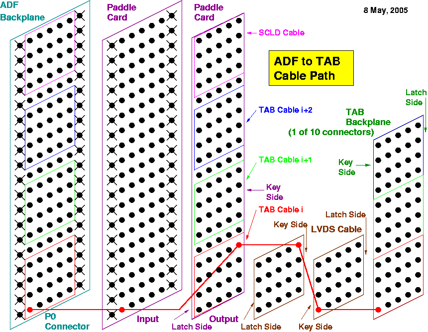
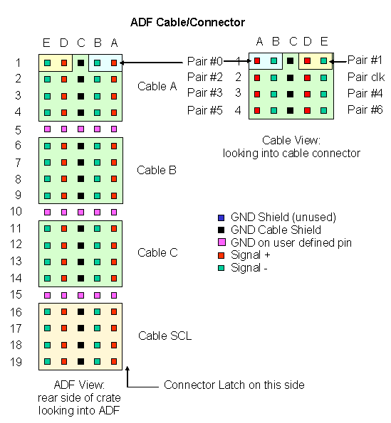
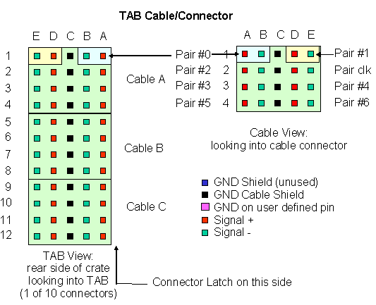
Cables & Connectors
Connector & Cable Diagrams
- ADF to TAB cable path
- through the transition system Paddle Card
- Cable and Connector Diagrams at the Boards
- ADF end
- TAB end
-
Note: the pin column labeling convention used in the
L1Cal diagrams above is opposite to that used in the AMP
cable spec given below: i.e. column A in the L1Cal
diagrams corresponds to column E in the spec.
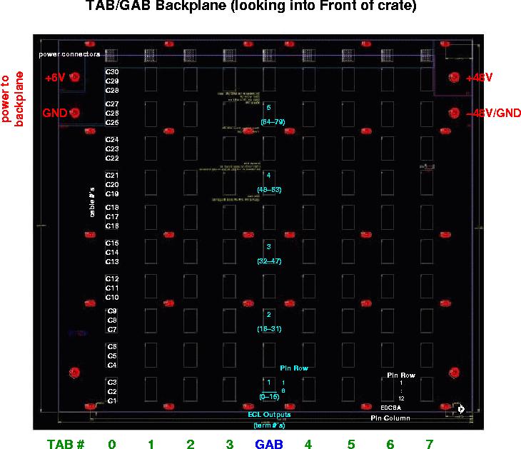
- TAB/GAB Backplane Connections
Cable Specifications
Transmitters & Receivers
Tests of the Cables
ADF to TAB Data Transmission Speed
LVDS Clock Speed
-
f(clock) = (7 streams/cable) x (8-bits/stream) / 132 ns
= 424 MHz
-
f(data) = (6 streams/cable) x (8-bits/stream) / 132 ns
= 364 MHz
Data Transmission Rate
- 1 ADF to TAB:
R(ADF) = (7 cables) x f(data) = 318 MByte/s
- 30 ADFs to 1 TAB:
R(TAB) = (30 ADF-cables) x R(ADF) = 9.5 MByte/s
- 240 ADF cables to 8 TABs:
R(tot) = (240 ADF-cables) x R(ADF) = 76 GByte/s